 |
|
|
|
|
|
|
|
|
|
|
|
|
|
|
|
|
|
|
|
|
|
|
|
|
|
|
|
|
|
|
| X-Ray Inspection - Technical Papers | ||||
|
||||
| Engineer's
fact File X-Ray Inspection X-ray technology has been used in printed circuit board (PCB) manufacturing since the emergence of multilayer boards in the early 1980s. The recent development of leadless devices having hidden solder joints, such as ball grid arrays (BGAs) and flip chips, has created a need for x-ray inspection in electronics assembly. Three basic types of x-ray imaging systems are used currently in the electronics industry. Film-based x-ray cabinets are the most cost-effective systems available. Real-time x-ray systems use an electronic x-ray camera to produce high-resolution images in real time. Industrial tomography systems, based on the same principles as their medical counterparts, can provide images of a single cross section of an object. The cost of an x-ray imaging system can range from £10,000 for a film cabinet to more than £500,000 for a tomography system. Despite the wide range in price, any of these x-ray systems can be used effectively to inspect PCBs and electronics assemblies. A real-time x-ray imaging system operates by illuminating an object with an x-ray source. The x-rays are absorbed and scattered as they pass through the object. An x-ray camera collects the remaining x-rays and displays an image. The lightest parts of the image occur where there is very little material to absorb the x-rays such as a drilled hole on a PCB. The darkest parts of the image occur where there is a large amount of absorbing material, such as at the solder ball of a BGA. Similar to a medical radiologist, the x-ray system operator learns by experience to interpret the x-ray image of a bare PCB or an assembled and soldered PCB. Most operators become proficient at interpreting an x-ray image within a few weeks. Inspection of PCBs Printed circuit board manufacturers use x-ray technology to inspect the inner layers of multilayer PCBs and to verify that the drilled holes are located properly. Inner layer misregistration can occur from improper alignment of the phototool or from a size change of the phototool material. The result is a shift of the pads and clearances from layer to layer in the multilayer PCB. X-ray technology provides a means to inspect solder joints in leadless packages Inner layer shift is identified easily in an x-ray image and a simple technique can be used to measure the misalignment precisely. In developing the PCB artwork, a set of non-overlapping coupons are placed around the outside of the panel. the coupons are test-drilled and examined in an x-ray system. Measurement of the hole location in each coupon allows the user to determine precisely the alignment of each of the inner layers as well as calculate the drill offsets for best hole position. X-ray inspection also is used to determine drilled hole location during production. PCBs can be inspected after tooling holes are drilled to verify that the tooling holes are in the proper locations. In addition, x-ray inspection can be performed after final drilling to verify that the holes are centered within the pads. The x-ray inspection system should be able to measure hole offsets so corrections can be applied during production. The emergence of leadless packages such as BGAs and flip chips has created a problem for assemblers: how to inspect the hidden solder connections after reflow. X-ray technology provides a means to monitor the assembly process as well as to check for solder defects within a BGA or flip chip (Fig. 1). |
||||
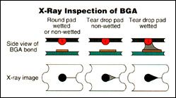 Figure 1: X-ray inspection Wetted or nonwetted on teardrop pad. |
||||
| It is generally
recognized that 100 percent x-ray inspection is not required for BGA assembly.
X-ray technology is most economical when applied as a tool for process
monitoring and control. Process monitoring is accomplished by visually
examining the x-ray image to verify solder ball size and shape uniformity
throughout the assembly. In addition, spot checks should be performed
to identify the more common defects in BGA assembly. X-ray inspection is an especially critical tool for rework of BGAs and flip chips, where the soldering process parameters are more difficult to control than on the assembly line. The x-ray image provides the rework operator with the information necessary to set and control the rework process parameters and to confirm that the component is attached properly. |
||||
| BGA and flip chip assemblies can suffer from the same common defects as conventional surface mount components. These defects include bridging, misalignment, missing balls, voids and opens. However, the defect rate for BGAs is reported to be 100 times smaller than for equivalent fine-pitch components. The possible defects are as follows: | ||||
| Bridging - Bridging (or shorts) occurs from excess solder that flows between adjacent solder balls. Bridging can occur because of excessive solder, or poorly cleaned stencils or PCBs. It is found more commonly in rework, where restenciling of the solder paste is more difficult. This defect, which is seen easily in an x-ray image, is the most common defect associated with BGA assembly. | ||||
| Missing balls - Missing balls can originate for the BGA foundry or can be caused by mishandling of the package. The absence of a solder ball is identified easily in the x-ray image. | ||||
| Misregistration - Misregistration between the solder balls and the pads on the PCB is an infrequent but potential assembly defect. In most cases, the surface tension of the molten solder will cause the BGA to self-align during reflow. Some case of misregistration have been seen in rework if the operator tried to hand-correct the alignment of a package before reflow. In rework, it is best to refrain from any x-ray examination before reflow. Misregistration is seen easily in the x-ray image, appearing as oval solder attachments. | ||||
| Voids - Voids are non-solder materials (such as flux) trapped within the solder joint. Voids can be caused by an inadequate reflow oven temperature profile that does not allow the flux to escape fully, or by contaminant materials as a result of poorly cleaned PCBs. There is currently a debate over the impact of voids. A recent study (Banks et al., Proc. SMI, 1996) indicates that small voids (less than 24 percent of the pad size) can actually increase solder joint reliability. Larger voids appear in an x-ray image as light spots within a solder ball attachment. | ||||
| Opens - Opens are breaks in the solder attach between a BGA and the PCB. The break can be caused by a crack in the solder or by insufficient solder. Opens are not detected directly using x-ray imaging. Visual and x-ray imaging, however, can be used to identify other symptoms associated with opens. Visual inspection can identify tilt or "potatochipping" of the BGA package, which can lead to opens. Computer analysis of the x-ray image also can help identify variations in solder ball size and shape related to insufficient solder or stress relief during reflow, either of which can produce opens. | ||||
| X-ray technology
is an integral part of electronic fabrication and assembly processes.
X-ray imaging technology is most cost-effective when employed as a tool
for process monitoring. David A. Zweig, Glenbrook Technologies, Inc., Morris Plains, N.J. Reprinted from Electronic Packaging Production May 1997 ©1997 by Cahners Publishing Co. |
||||


